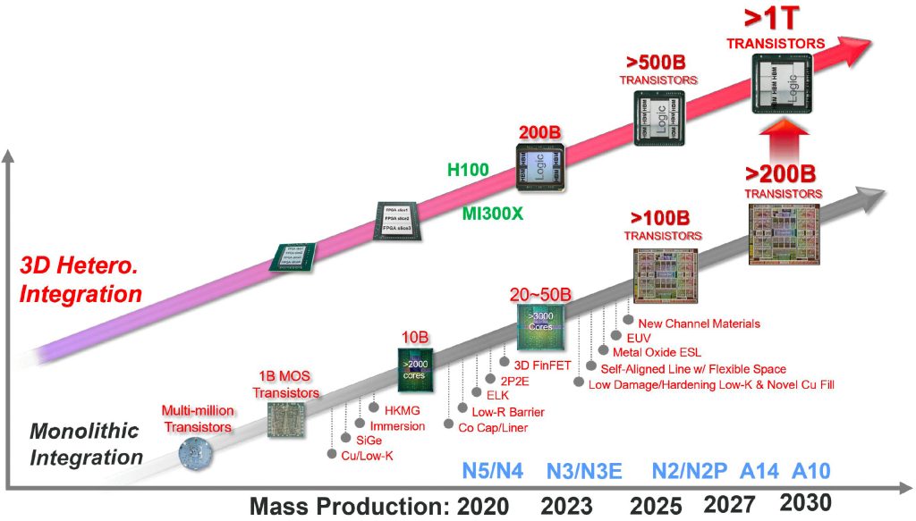
At IEDM, TSMC shared its plans to provide MCM-based chips with over one trillion transistors and monolithic chips with over 200 billion transistors by 2030. To accomplish that target, the company said it is working on 2nm-class N2 and N2P production nodes, as well as 1.4nm-class A14 and 1nm-class A10 manufacturing processes, all due by 2030.
TSMC is optimistic that it will develop its next-generation production nodes over the next five to six years, even though process technology development has slowed down in recent years as chipmakers encounter technical and financial challenges. The company faces the same obstacles as other firms, but it is confident in its abilities as the world's largest foundry.

TSMC predicts that even more complex monolithic circuits with over 100 billion transistors will be available shortly, as Nvidia's 80-billion-transistor GH100 remains one of the most complicated monolithic processors on the market. However, building such massive processors becomes more complex and costly, leading many organisations to adopt multi-chiplet architectures, such as AMD's Instinct MI300X and Intel's Ponte Vecchio.
According to TSMC, this trend will continue, and in a few years, we will witness multi-chiplet systems with over a trillion transistors. To achieve that, TSMC anticipates breakthroughs in packaging technologies, too. At the same time, monolithic chips will become more complex, with monolithic CPUs comprising 200 billion transistors.
KitGuru says: Although the development of new process nodes is slowing down, it's nice to see that, at least up to 2030, there are plans to keep increasing transistor density at a steady pace.
The post TSMC expects to create chip packages with over 1 trillion transistors by 2030 first appeared on KitGuru.
0 comments :
Post a Comment